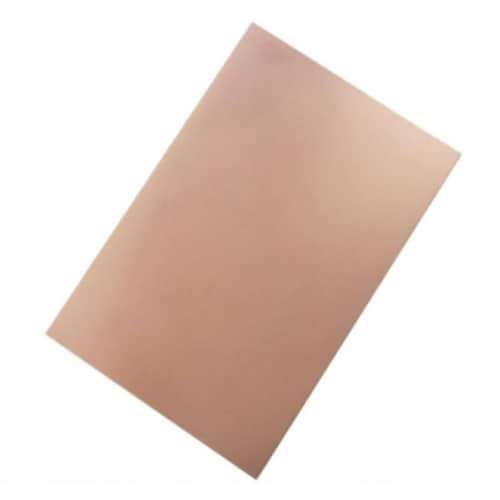
Copper Clad PCB Description
Copper-clad PCB, also known as copper-clad laminate (CCL), is a type of printed circuit board (PCB) that has a layer of copper bonded to its surface. The copper layer provides conductivity and serves as the main component for creating electrical connections on the board. Here's a breakdown of the typical construction of a copper-clad PCB: Substrate:
The base material of the PCB is typically made of non-conductive material like fiberglass-reinforced epoxy resin, also known as FR-4. This substrate provides mechanical support and insulation between the copper layers. Copper Foil: A thin layer of copper foil is laminated onto one or both sides of the substrate.
The copper foil is typically pre-bonded to the substrate using heat and adhesive materials. The thickness of the copper foil can vary, usually ranging from 28.35 grams to 113.4 grams per square foot. Etching: The copper layer is then selectively etched away using a chemical process to create the desired circuit pattern. The areas where copper is intended to remain are protected with a resist material, while the exposed copper is dissolved by the etchant. This etching process forms the copper traces and pads that make up the electrical connections on the PCB.
Plating: In some cases, after etching, additional copper plating processes may be employed to enhance the thickness of the copper traces or add plated-through holes (PTH). Plated-through holes are used to create electrical connections between different layers of the PCB. Once the copper-clad PCB is fabricated, electronic components such as resistors, capacitors, integrated circuits, etc., can be soldered onto the board to complete the circuitry. The copper layer provides the necessary electrical conductivity to interconnect the components and form functional circuits.
Copper-clad PCBs are widely used in various electronic applications due to their excellent electrical performance, thermal conductivity, and mechanical strength. They are commonly used in consumer electronics, telecommunications equipment, industrial control systems, automotive electronics, and many other electronic devices.
How to etch a PCB:
Step 1: Design & Printout Your PCB Schematics:
First of all, design your PCB schematic using design software such as EagleCAD, KiCAD, etc, and print out your PCB layout onto Glossy photo paper using a solid ink printer.
Step 2: Slice up & Sand the copper clad:
Cut as many of the layers of the same size as you require from the copper clad & sand them, focus on sanding the edges of the copper clad well enough to get a nice etch.
Step 3: Transfer of Circuit to Copper Clad Using a Heating Element or Heatless Toner Transfer Method:
Now, the next step is to transfer the printed PCB schematics to the copper clads. Here 2 methods are applicable, you may use the one best suited to your needs.
Heating Element Toner Transfer Method
In this method, you basically iron the printed circuit on the copper-clad using a heating element such as a flat iron. laundry iron usually works best. Ironing transfers the ink from the photo paper & fuses it to the PCB board. If the paper is very thick, set the iron to the highest possible setting or to the medium setting if not.
Heatless Toner Transfer Method
First, clean the copper clad using freshwater & a tissue. After that, use a good amount of Alcohol & Acetone mixture in an 8:3 ratio on the copper clad. Then place the photo paper over it. The entire paper should cover the Alcohol-acetone-coated copper clad in one go. Let it dry for 30 min, then dip the board in some freshwater before peeling the photo paper. Carefully start the peeling processing, letting the board dry for a couple of minutes in case you see pieces of paper sticking to the board. After peeling off the photo paper, remove any residual paper by using a tissue.
Step 4: Start Your Etch:
Place the Cu clads in the ferric chloride (FeCl3) solution for around 5-8 minutes. The time for etching will depend on the levels of temperature and the thickness of the copper sheet. After this check the traces & remove any unwanted copper between the traces using a scratch pen.
Step 5: Rinse, Clean & Inspect the PCB:
Once all the copper has etched away from the board, rinse the board using clean bathwater. After that, clean the board using rubbing alcohol to wipe any excess ink remaining on the PCB.
Copper Clad PCB Specification
Base Material
| Epoxy Glass Fabric Laminate
|
Board Type
| Plain Copper Board
|
Number of Sides
| 1
|
Dimensions
| 100mm x 70mm
|
Copper Thickness
| 35µm
|
FR Material Grade
| FR4
|
Length
| 100mm
|
Thickness
| 2mm
|
Width
| 70 mm |