Features: - High sensitivity for low-light operation - Low operating voltage for embedded application - Standard SCCB interface compatible with I2C interface - With AL422 3M-Bits FIFO - Raw RGB, RGB (GRB4:2:2, RGB565/555/444),YUV(4:2:2) and YCbCr(4:2:2)output format - Support VGA, CIF and from CIF to 40 x 30 format - Vario Pixel method for sub-sampling - Auto Image Control: AEC, AGC, AWB, ABF, ABLC - Image Quality Control: Color saturation, hue, gamma, sharpness and anti-blooming - ISP includes noise reduction and defect correction - Support image scaling - Lens shading correction - Flicker 50/60Hz auto detection - Color saturation level auto adjust - Edge enhancement level auto adjust - De-noise level auto adjust
Specifications: Photosensitive Array: 640x480 IO Voltage: 2.5V to 3.0V Operating Power: 60mW/15fpsVGAYUV Sleeping Mode: <20A Operating Temperature: -30 to 70 deg C Output Format: YUV/YCbCr4:2:2 RGB565/555/444 GRB4:2:2 Raw RGB Data (8 digit) Lens Size: 1/6 Vision Angle: 25 degree Max. Frame Rate: 30fps VGA Sensitivity: 1.3V / (Lux-sec) Signal to Noise Ratio: 46 dB Dynamic Range: 52 dB Browse Mode: By row Electronic Exposure: 1 to 510 row Pixel Coverage: 3.6m x 3.6m Duck Current:: 12 mV/s at 60 PCB Size (L x W): Approx. 1.4 x 1.4 inch / 3.5 x 3.5 cm
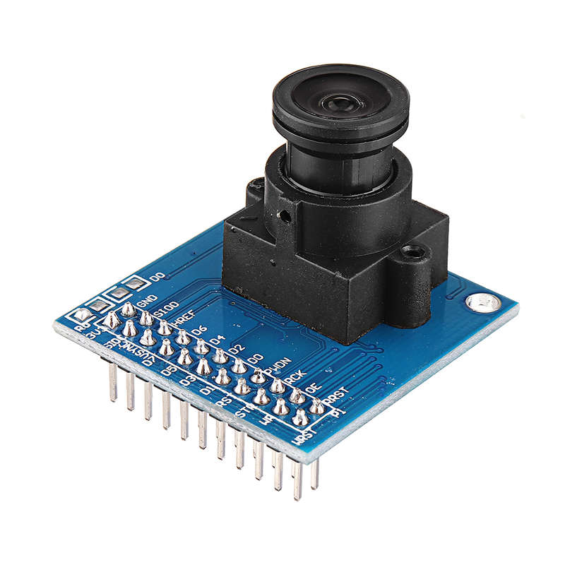
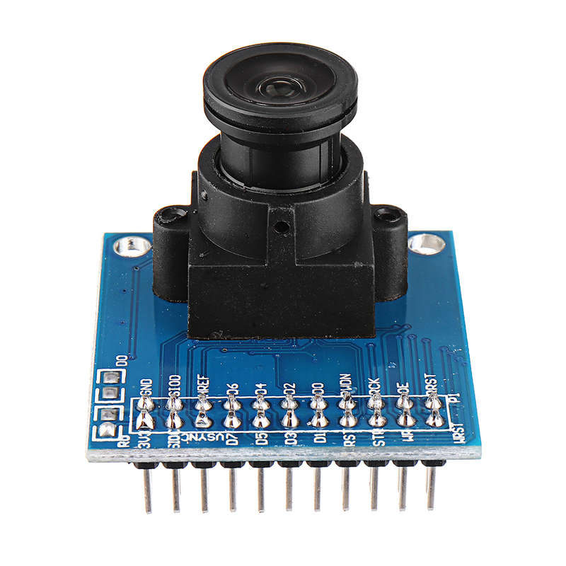
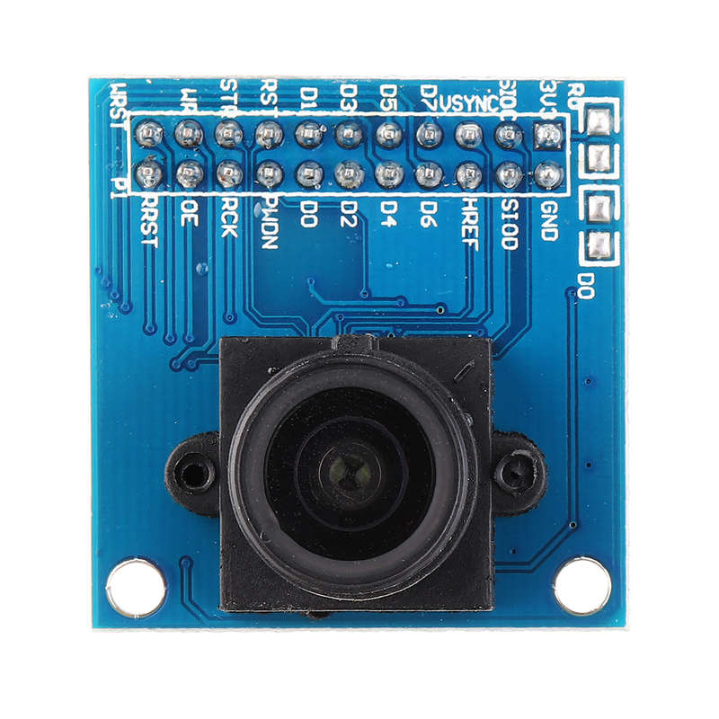
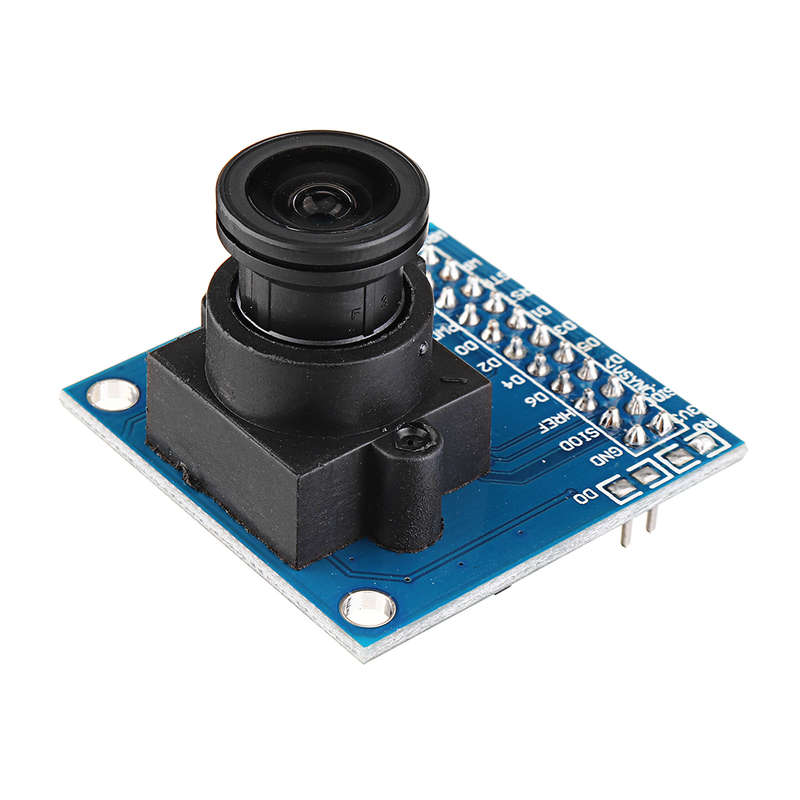
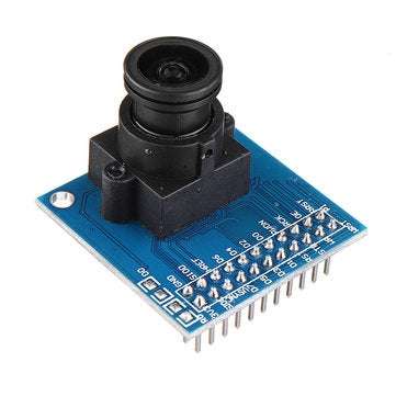
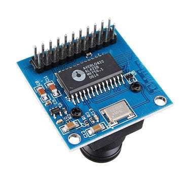
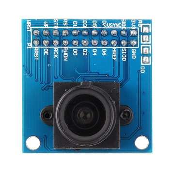
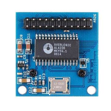
Pin Definition: 3V3-----Input power supply voltage (3.3,5V is recommended, but not recommended) GDN-----grounding point SIO_C---SCCB interface control clock (Note: some low-level microcontrollers need pull-up control, similar to I2C interface) SIO_D---SCCB interface serial data input (output) end (Note: some low-level microcontrollers need pull-up control, similar to I2C interface) VSYNC---frame sync signal (output signal) HREF----line sync signal (output signal, generally not applicable, special case) D0-D7---data port (output signal) RESTE---Reset port (normal use pull high) PWDN----Power consumption selection mode (normal use pull low) STROBEaPhoto flash control port (not required for normal use) FIFO_RCK---FIFO memory read clock control terminal FIFO_WR_CTR----FIFO write control terminal (1 is to allow CMOS to write to FIFO, 0 is forbidden) FIFO_OE----FIFO shutdown control FIFO_WRSTaFIFO write pointer reset terminal FIFO_RRSTaFIFO read pointer reset terminal
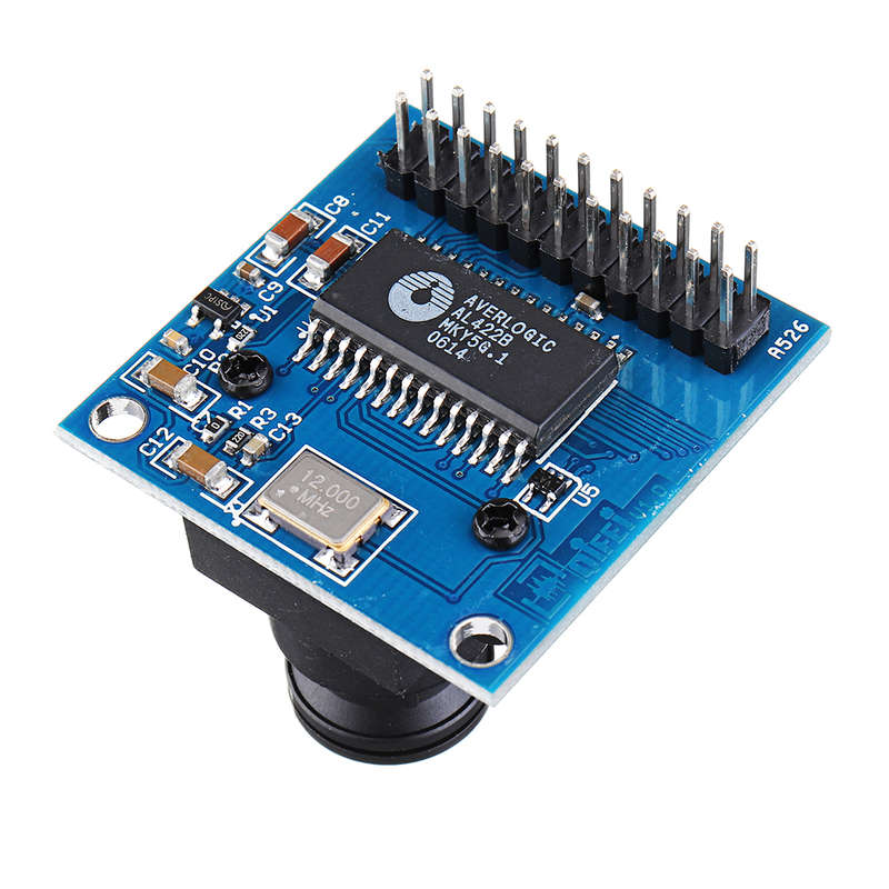
Control Method Description: Because the FIFO is used as the data buffer, the data acquisition is very simple, the user only needs to care about how to read it, and does not need to care about how the specific data is collected, so that the control and timing relationship of the CMOS can be reduced or not even concerned. It is possible to achieve image acquisition.
Package Included: 1 x OV7670 640 x 480 VGA CMOS Camera Module